
Gallium Nitride Horizontal

CNC
The present invention provides a transverse epitaxial growth method of gallium nitride and a compound semiconductor thereof. Firstly, a layer of characteristic silicon nitride grows on a substrate surface of sapphire (0001) or silicon (111) or silicon carbide (0001) by adopting organic matter chemical vapor deposition or molecular beam epitaxy or hydride vapor deposition, and subsequently, a ...


Brillouin stering study of gallium nitride: elastic ...
Gallium nitride is one of the major semiconductors that have been under extensive theoretical and experimental investigation over the past few years [1–4]. ... The horizontal line shows the direction of the c axis. The solid line indies the direction of incident light and the broken line indies the direction of stered light. In ...


SteadyState Empirical Model for Electrical Activation of ...
Index Terms—Gallium nitride, implantation, annealing, electrical activation, power devices, modeling I. INTRODUCTION Gallium nitride (GaN) is highly attractive for power electronic devices, due to its excellent material properties, in particular its wide bandgap (3:4eV) [1]. Even though GaN based devices which employ horizontal current ...

Properties and Appliions and Gallium
08/08/2019 · 5 Properties of Gallium. 1. Color Physical State: By its nature, Gallium is a kind of soft metal with a bluewhite color combination. Apart from mercury, rubidium, and cesium, it is the only metal that turns to liquid at room temperatures, making it possible to .

Raman Imaging of a Single Gallium Nitride Nanowire
of the widebandgap gallium nitride (GaN) are prime candidates for nanoscale devices such as short wavelength emitter optoelectronic devices and highpower/hightemperature electronics. Subsequently, it is ... horizontal part of the nanowire. China: 3/3 Semiconductor 04 Figure 3: ...


Wide Bandgap Semiconductor Laboratory
He is the coeditor of eight books, including Gallium Nitride I (Academic Press, 1998) and Gallium Nitride II (academic Press, 1999), the author of chapters in eight books and 340 papers in technical journals and conference proceedings (Google citations 11,550, h index 52). ... This horizontal hydride vapor phase epitaxy system is simpler and ...


AIXTRON Global Presence
based on the principle of horizontal laminar flow. The required process ... Gallium Nitride (GaN). These semiconductors are the most im ... Ga = Gallium In = Indium N = Nitrogen P = Phosphorus As = Arsenic Sb = Antimony 9,0 Be II III Pe riod e IV VV I 4 10,8 B 5 12,0 C 6 14,0 N 7


Continuation: Obtaining and characterization of gallium ...
16/04/2007 · The compounds were prepared in horizontal quartz reactor. As a source of gallium, metallic gallium or gallium nitride powder were used and as a source of nitrogen gaseous ammonia was used. This study has been undertaken in order to determine the influence of process conditions on growth of gallium nitride single crystals, monolayers and ...


Fundamentals of Gallium Nitride Power Transistors
The threshold of gallium nitride transistors is lower than that of silicon MOSFETs. This is made possible by the almost flat relationship between threshold and temperature along with the very low C GD, as described later. Figure 3 shows the transfer characteristics curve for .


Effect of Au/SiO2 substrate on the structural and optical ...
gallium nitride, the influence of the substrate on the crystalline, electron, optical and compositional properties of the ... Schematic diagram of the CVD horizontal reactor used for the growth of GaN films on Au/SiO2 and Si substrates. resolution images and interplanar distances were obtained for GaN films. To study the crystalline ...


Gallium Nitride
Gallium nitride is a IIIV semiconductor and has very high chemical resistance to corrosive environments. Strong bond existing between Ga and nitrogen is responsible for the corrosion resistance properties the compound. Bulk gallium nitride is a direct band gap semiconductor (band gap = eV) having wurtzite type structure and is the material used for making lightemitting devices that can ...


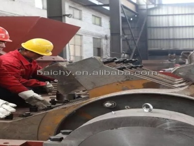
gallium nitride horizontal
gallium nitride horizontal. Home / Products. Gallium Nitride an overview ScienceDirect Topics. Gallium nitride (GaN) as an IIINitride is a widebandgap semiconductor and has found many appliions in optoelectronics One of its most known appliions is the GaNbased violet laser diode used to read Bluray Discs Also, many of the LEDs are based ...

It's Time to Rethink Power Semiconductor Packaging
11/03/2019 · When people think of wide bandgap power semiconductors, they are usually thinking of gallium nitride (GaN) or silicon carbide (SiC). This article will focus on lower voltage GaNonSi power device packaging because that is where designers of power systems are most pressed to reduce system size, cost, while increasing efficiency and power density.


Horizontal Assembly of Single Nanowire Diode Fabried by ...
The transport studies of horizontal gallium nitride nanowire structures assembled from p and ntype materials show that these junctions correspond to welldefined pn junction diodes. The pn junction devices based on GaN nanowires suspended over the electrodes were fabried and their electrical properties were investigated. The horizontally ...


Lowcost Fabriion of Tunable Band Gap Composite Indium ...
19/02/2019 · HighBrightness Light Emitting Diodes Using DisloionFree Indium Gallium Nitride/Gallium Nitride MultiquantumWell Nanorod Arrays. Nano Lett. 4, 1059–1062 (2004). ADS CAS Article Google Scholar
SUBSTRATES FOR EPITAXY OF GALLIUM NITRIDE: NEW .
Gallium nitride constitutes solid solutions both with aluminum nitride (AlN) and indium nitride (InN) providing a very wide range of energy band gap ( eV). Such ability to build up solid solutions plays a key role in construction of shortwave emitters and heterostructures with high potential barrier. In addition, gallium nitride pos

SteadyState Empirical Model for Electrical Activation of ...
Index Terms—Gallium nitride, implantation, annealing, electrical activation, power devices, modeling I. INTRODUCTION Gallium nitride (GaN) is highly attractive for power electronic devices, due to its excellent material properties, in particular its wide bandgap () [1]. Even though GaN based devices which employ horizontal current ...

Advantages of Using Gallium NitrideFETs in Satellite ...
horizontal through the GaN 2dimensional electron gas (as shown by "–" in the diagram). Figure 1. EPC's GaN Power Transistor Structure GaN is a wide bandgap material. Compared with silicon, the separation between the drain and source ... White Paper – Gallium Nitride .


10000V! New record for breakdown voltage of GaN power ...
11/06/2021 · The gallium nitride epitaxial material structure used to realize this new device includes 20nm p+GaN/350 nm pGaN cap layer and 5 channels of 23nm /100nm GaN intrinsic layer. The epitaxial structure was realized by the Suzhou Jingzhan team through a single continuous epitaxy on a 4inch sapphire substrate through the MOCVD method ...


Lightemitting diodes with surface gallium nitride p–n ...
01/03/2019 · Commercial WLEDs are mainly produced by combining gallium nitride (GaN)based blue LED and yellow phosphor or combining red, green, and blue LEDs. ... Current spreading in the horizontal direction ...


Topdown fabriion of horizontallyaligned gallium ...
01/07/2015 · 01/07/2015 · This paper describes a method for mass production of CMOS compatible gallium nitride (GaN) nanowire (NW) arrays for sensors and other appliion. The method uses a topdown etching technique starting from a thinfilm GaN layer. The etching process on a fixed substrate creates the horizontally aligned GaN NWs.