
Pcb Fabriion Steps Ppt
PPT – PCB Manufacturer PowerPoint presentation | free to ...
Steps in PCB Circuit Board Manufacturing 1)Film Generation 2) Select Raw Material 3)Drill Holes 4)Electroless Copper 5)Apply Photoresist and Image 6) Pattern Plate 7) Strip Etch 8) Soldermask 9)Nomenclature(silkscreen) 10)Surface Finish Applied 11)Fabriion. – PowerPoint PPT presentation

fabriion process of iron ppt
fabriion process of iron ppt. Nov 27 2013 · Cast iron 1 Gulfam Hussain egulfam 2 Cast Iron is generally defined as an alloy of Iron with 2 to 45 Carbon and usually with more than 01 Silicon The three main ingredients are Iron Carbon Silicone Cast iron containing more of these materials than steel... As a leading global manufacturer of crushing equipment, milling equipment ...
PCB Designing Using Circuit Maker(Altium) : 3 Steps ...
Step 2: PCB Footprint. Click Project>Add New PCB. In Footprint,click Project>Import Changes from Click Ctrl+A to select all components drag It into the board and place as per requirement (prevent overlap and keep components close to each other) Click Route under Home Tab and track the component or click Autoroute under Tool Tab.

Printed board circuit design (Pcb) PPT
· PCB FLOW 7. LIBRARY CREATION OF COMPONENTS IN ORCAD We have to create each and every component in library. 8. PCB DESIGNING PROCESS Step by step: Schematic design: It is a circuit diagram. It uses agreed symbols to represent components and show how they area electrically connected. 9. ENTERING PCB FOOTPRINT FILE CREATE NETLIST 10.

KiCad Tutorial: Make Your First Printed Circuit Board
· In this KiCad tutorial for beginners, you'll learn to make your first Printed Circuit Board (PCB). You'll get simple stepbystep instructions on how to draw schematics, board layout, and getting your board made cheaply.

PCB Manufacture: How are PCBs Made » Electronics Notes
With the bare PCB boards chosen and available the next step is to create the required tracks on the board and remove the unwanted copper. The manufacture of the PCBs is normally achieved using a chemical etching process. The most common form of etch used with PCBs is ferric chloride. In order to gain the correct pattern of tracks, a photographic process is used. Typically the copper on the ...

PCB Assembly Process
The first step in the actual PCB Assembly process is the appliion of solder paste to the bare PCBs. Here the stainlesssteel stencil that was created during PCB Fabriion is fit over the bare board, leaving only the pads for assembly of surfacemount components uncovered. The stencil is held in place by a mechanical fixture, and an ...
PCB Manufacturing ProcessHow to make PCB,Fabriion ...
For PCB fabriion, some basic steps have to be followed. The detailed description on how to make PCB is explained below. The step by step procedure can be obtained by checking the following links. PCB Etching Process | PCB Drilling | Conductor Plating | Solder Resist | PCB Testing | PCB Assembling . Take a look at the video below to get a brief idea about how a PCB is made. Once you have ...

Plated through hole(PTH) in PCB fabriion
Plated through hole(PTH) in PCB fabriion 8775 0 Aug, 10:44:31 Return. Plated through hole(PTH) in PCB fabriion . There is a confusion about whether is conductive or not between two sides circuit board or multilayer circuits as the base material only has copper foil on both sides, and insulating layers is in the middle. What's more, how to connect with the two side circuit to ...

Printed Circuit Board Assembly – PCBA Design ...
Mar 04, 2021 · A Printed Circuit Board (PCB) is a Board made of different heat resistant insulating materials. Conductive copper tracks are printed or etched onto this conconductive base substrate. Electronic components are then soldered onto this board making it a Printed Circuit Board .
![4 Methods To Recover Previous Version Of PowerPoint[2021]](/i7ud2wy/1184.jpg)
![4 Methods To Recover Previous Version Of PowerPoint[2021]](/i7ud2wy/791.jpg)
4 Methods To Recover Previous Version Of PowerPoint[2021]
Follow these simple steps to recover previous versions of your PowerPoint presentation files using PowerPoint. Step 1. Open the current version of the PowerPoint presentation file, and tap on "File" on the top left of your screen. Step 2. From the list of options displayed at the top of your screen, click "Browse Version History" to loe the previous versions of the PowerPoint ...


EE261 Lecture Notes (electronic)
PCB: Vias. Vias (Drilling) A via is a structure that electrically connects two different layers of copper in a PCB. the first step in creating a via is to drill a hole where the contact will be made. this can be done using: 1) A mechanical process (, a regular drill bit). This .


PCB Fabriion Process20 Steps Ultimate Guide On PCB ...
PCB Fabriion Process employs many new areas of technology that have led to significant improvements in reducing the size of the components and rails used and the reliability of the board. Producing a PCB is a complex process that involves many steps. Here, we will introduce you to the entire PCB fabriion process of our factory. It has 20 ...
PCB Assembly and Production Process » Electronics Notes
The PCB assembly process for the manufacture of loaded printed circuit boards has been considerably simplified in this overview. The PCB assembly and production processes are generally optimized to ensure very low levels of defects, and in this way produce the highest quality product. In view of the number of components and solder joints in today's products, and the very high demands placed on ...

PFMEA Process Failure Mode and Effects Analysis
The process must be defined step by step, including interfaces The PFD provides the structure to document what product characteristics and requirements (OUTPUTS) are affected by a given operation and how these characteristics and sources of variation are controlled (INPUTS) PFD is a graphical representation of every possible path a part can take through the anticipated manufacturing process A ...

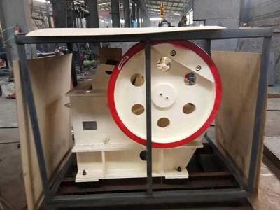
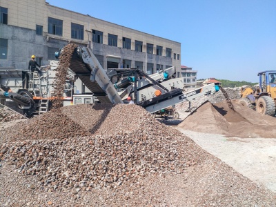
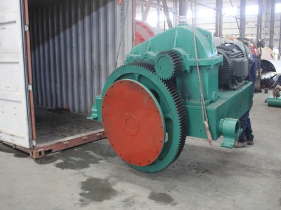
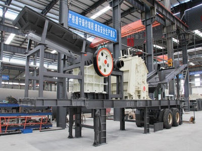
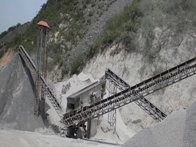
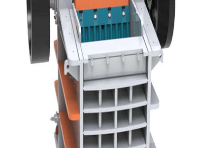
ton
Ton Cone Crusher Magnetic Separator; Ton Medical Equipment Inc Careers In Computer Literate; Ton Impact Crusher Old; Ton Jaw Crusher Maintenance; Ton Jaw Crushers Housing

AN Appliion Note RF Design Guidelines: PCB ...
This appliion note describes step by step techniques for ensuring the correct PCB layout and subsequent design optimization steps for each circuit block of the RF integrated circuit architecture. Figure 1: Semtech Transceiver Architecture 1 Reference design files for Semtech's XE/SX1200 RF ISM band ICs can be obtained by contacting sales VDDF VSSF VDDP VSSP VDDA VSSA .